GPU Compute and Memory Architecture
In this blog post, I start with a brief discussion of the modern GPU architecture, which includes the memory hierarchy. I then spend considerable time on how the CUDA software constructs interact with the actual hardware.
So far, in chapters 1 and 2, I have given a high-level overview of CPUs, GPUs, and the GPGPU programming model (CUDA) using vector addition and simple matrix multiplication as examples. I explained how to write functions that can run directly on the GPU. Ultimately, the goal was to speed up applications, and for matrix multiplication, I achieved 2678x improvement over the sequential version that runs on a CPU. This was an amazing result, but the problem size in this example was quite large (matrices of size 8000 x 8000). It would be interesting to see how the computations on a GPU scale with more modest problem sizes. Figure 1 shows the matrix multiplication on a CPU and GPU for matrices of size ranging from 64 to 2048.
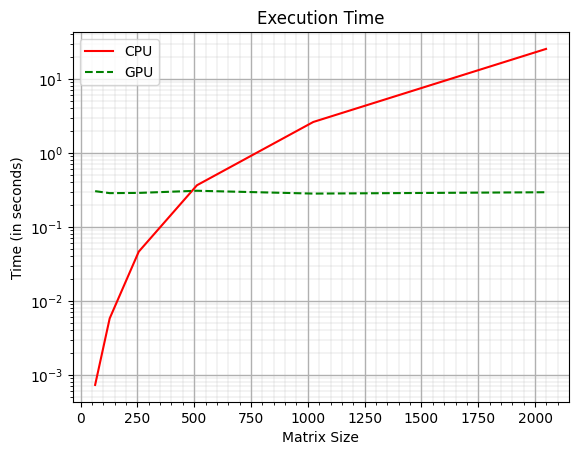
From Figure 1, you can see that for smaller matrices, the CPU is magnitudes faster than the GPU. It's only around the matrix size of 500 that the CPU execution time exceeds that of the GPU, and from what I have discussed so far, I can not answer why this is happening. Whenever something like this happens, it's always a good idea to go back to the fundamentals and start from there. In this case, that would be the GPU hardware!
The main objective of this blog post is to explain different hardware concepts essential for CUDA C programmers to understand and reason about the performance of their code. I will do this by answering five simple questions.
- What is the architecture of a modern GPU?
- What are the different memory types in a GPU?
- How do CUDA blocks/threads work with different GPU hardware components?
- What are the common coding practices to get the best out of a GPU?
- Is there a way to determine the resources available on a GPU?
Modern GPU Architecture
Figure 2 shows a high-level CUDA C programmer's view of a CUDA-capable GPU's architecture. There are four key features in this architecture:
- The GPU is organized into an array of highly threaded streaming multiprocessors (SMs).
- Each SM has several processing units called streaming processors or CUDA cores (shown as green tiles inside SMs) that share control logic.
- The SMs also contain a different on-chip memory shared amongst the CUDA cores inside the SM.
- GPU also has a much larger off-chip memory, the main component of which is the global memory or VRAM.
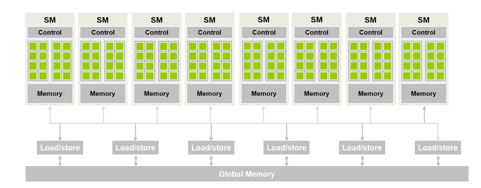
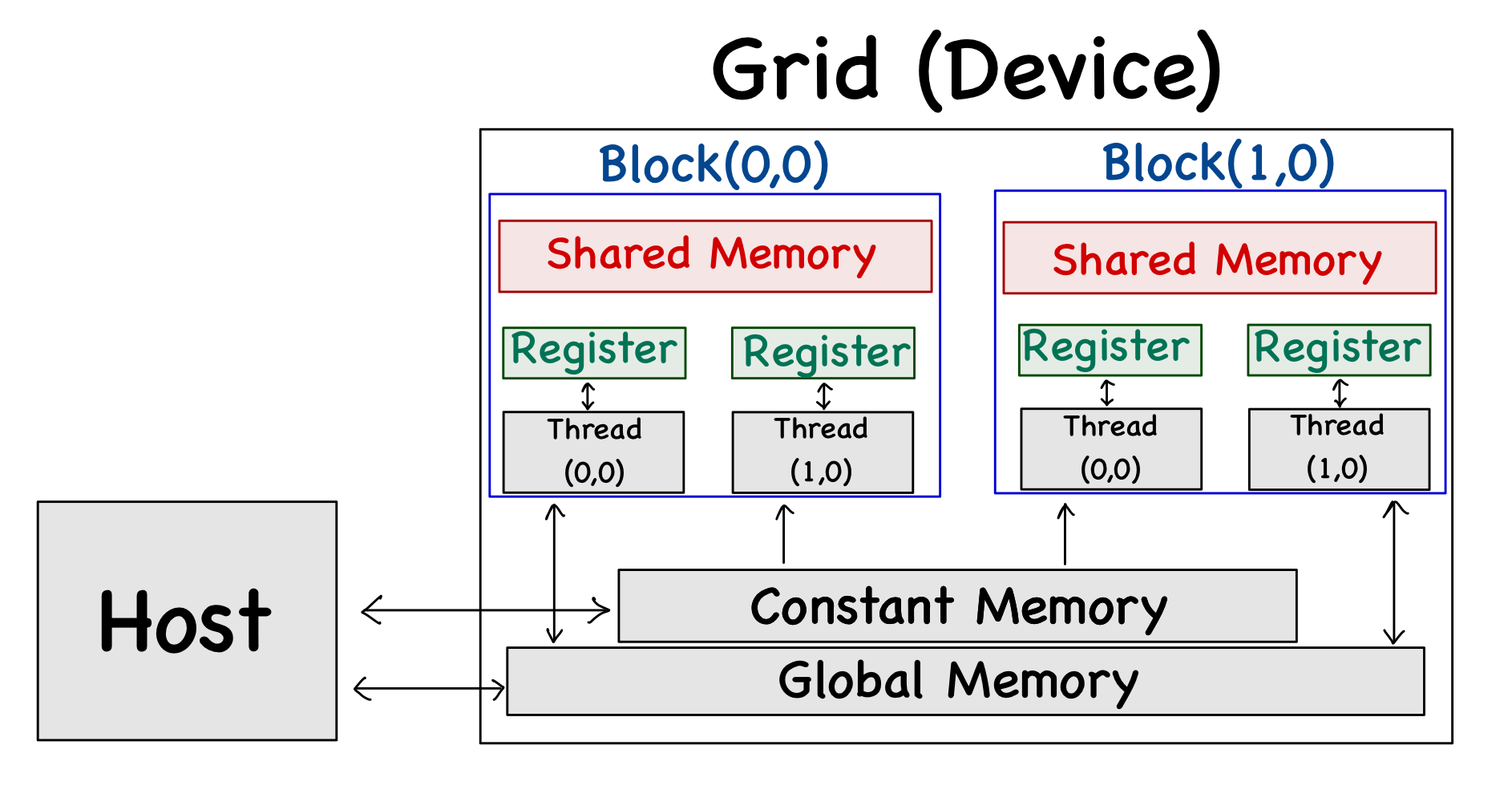
Figure 3 shows the on-chip and off-chip memory units alongside the threads, and the discussion related to the properties (like size, access latency, etc.) of these memory units is presented next.
Off-Chip Memory
Off-chip memory, as the name suggests, resides off the chip or relatively far away from where the cores are. There are three main types of off-chip memory units in a GPU.
- Global Memory
It is a large memory space (~24 GB) that resides off-chip. The purpose of this memory is to store large amounts of data, and for this reason, it has long latency and low bandwidth (the priority is the memory size, not the access speeds). Both CPU and GPU can read from and write to this memory. On the software level, all threads in the grid can access this memory.
- Local Memory
Local memory is placed inside global memory. It is similar to global memory but can only be used by a single thread. Each thread has its share of local memory where it can place data private to the select thread.
- Constant Memory
It is a small memory space (~64 KB) that resides off-chip. A CPU can write to and read from constant memory, but a GPU can only read from it (can not write to this memory unit). Despite being off-chip, constant memory has short latency and high bandwidth (it achieves this using some caching mechanism). On the software level, just like global memory, all threads can access it.
On-Chip Memory
On-chip memory units reside near the cores. Hence, data access from on-chip memory is blazing fast. The issue in this case is that the size of these memory units is very small (maximum of around 16KB per SM). There are two main types of on-chip memory units that we can manage with code.
- Shared Memory
Shared memory is a small memory space (~16KB per SM) that resides on-chip and has a short latency and high bandwidth. On a software level, it can only be written and read by the threads within a block.
- Registers
Registers are extremely small (~8KB per SM) and extremely fast memory units that reside on-chip. On a software level, it can be written and read by an individual thread (i.e., private to each thread).
All memories have different functionalities, latencies, and bandwidth. It is important to understand how to declare a variable to ensure that it resides in the intended type of memory.
| Variable Declaration | Memory | Scope | Lifetime |
|---|---|---|---|
| Automatic variables (except arrays) | Register | Thread | Grid |
| Automatic array variables | Local | Thread | Grid |
__device__ __shared__ int var; |
Shared | Block | Grid |
__device__ int var; |
Global | Grid | Application |
__device__ __constant__ int var; |
Constant | Grid | Application |
All this might feel a bit too overwhelming. So, here are the key points to remember when writing an application:
- When copying data from the host, it goes into global memory. Accessing data from global memory is computationally intensive.
- Shared memory access is faster than global memory, but it's small in size.
- Register memory access is blazing fast (usually two orders of magnitude faster than global memory), but it's even smaller in size.
Hardware-Software Interactions
Thread Blocks and SMs
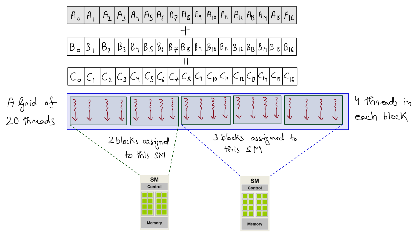
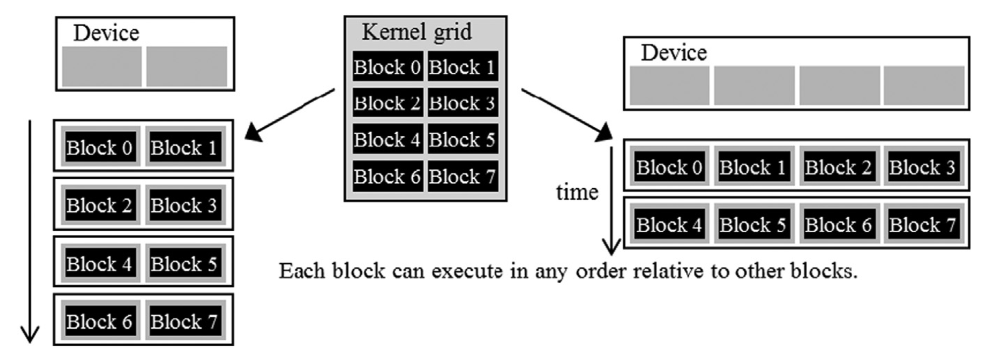
When a kernel is called, the CUDA runtime system launches a grid of threads that execute the same kernel code. These threads are assigned to SMs on a block-by-block basis, i.e., all threads in a block are simultaneously assigned to the same SM. Consider the vector addition example where vectors are of length 17, and a grid is launched such that each block has 4 threads (with a total of 5 such blocks). Multiple blocks will likely get simultaneously assigned to the same SM. For example, 2 different SMs could end up with 2 and 3 blocks, respectively.
The example discussed above is quite small. In real-world problems, there are a lot more blocks, and to ensure that all blocks get executed, the runtime system maintains a list of blocks that did not get assigned to any SM and assigns these new blocks to SMs when previously assigned blocks complete execution. This block-by-block assignment of threads guarantees that threads in the same block are executed simultaneously on the same SM, which:
- Makes interaction between threads in the same block possible.
- Allows (shared) memory to be shared between threads in the same block.
For a moment, it might look like an odd choice not to let threads in different blocks interact with each other. However, this feature allows different blocks to run independently in any order, resulting in transparent scalability where the same code can run on different hardware with different execution resources. This, in turn, reduces the burden on software developers and ensures that with new generations of hardware, the application will speed up consistently without errors.
Warps
In the previous section, I explained that blocks can execute in any order relative to each other, but I did not say anything about how threads inside each block are executed. Conceptually, the programmer should assume that threads in a block can execute in any order, and the correctness of the algorithm should not depend on the order in which threads are executed.
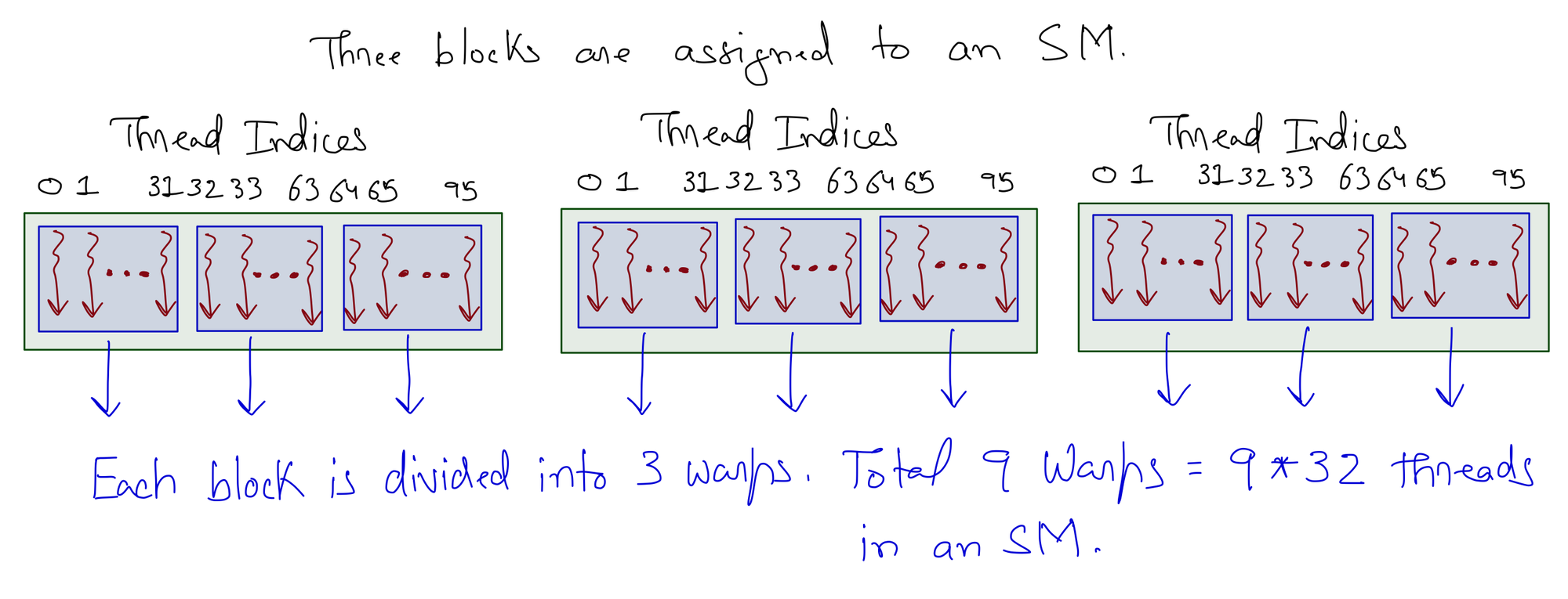
Thread scheduling in CUDA GPUs is a hardware implementation concept that varies depending on the type of hardware used. In most implementations, once a block is assigned to an SM, it is divided into 32-thread units called warps. The knowledge of warps is useful for understanding and optimizing the performance of CUDA applications.
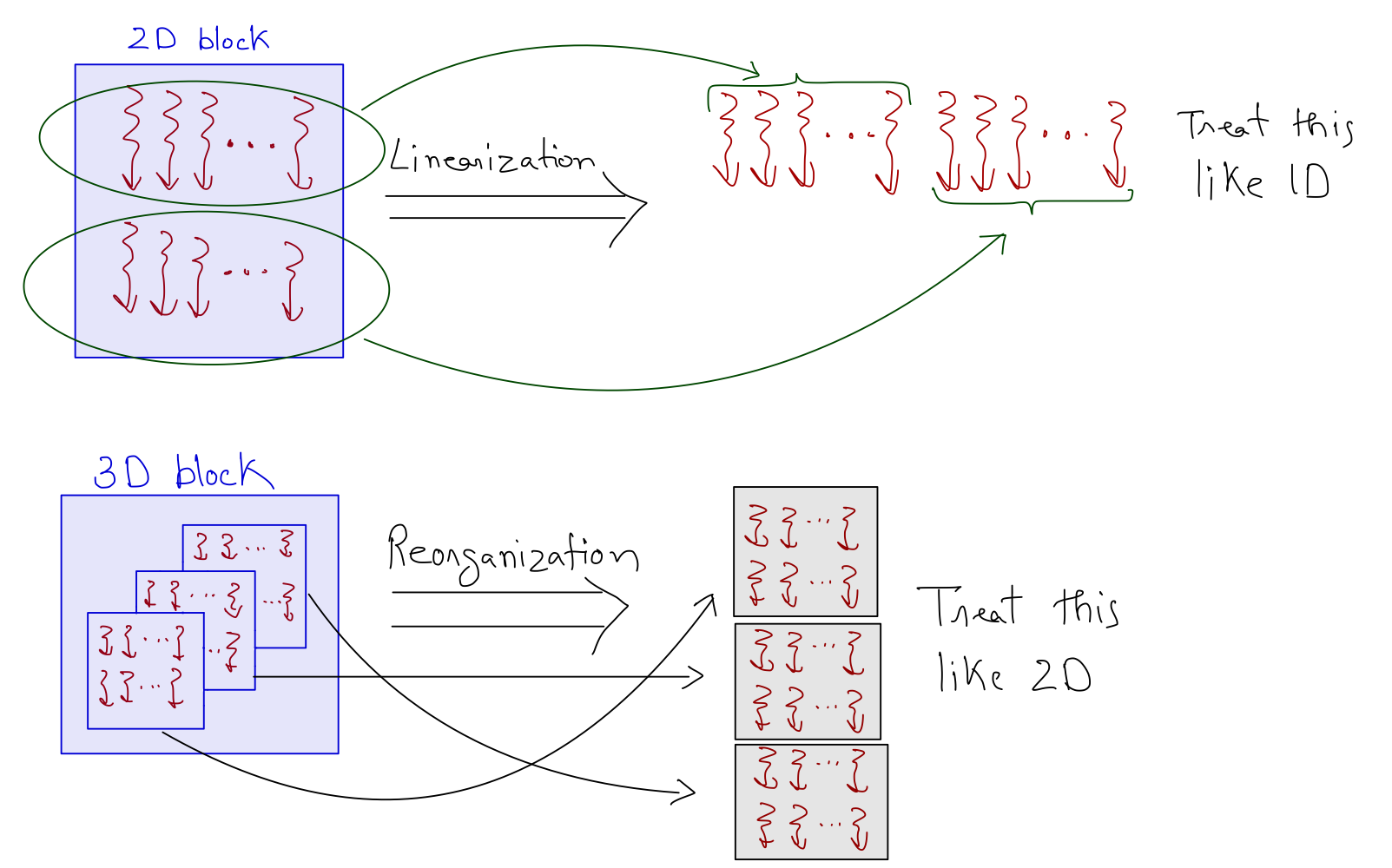
Each warp consists of 32 consecutive threads. For 1D block, this is straightforward such that threadIdx.x is used to divide the threads into warps.
For the 2D block, threads are linearized using a row-major layout and partitioned into warps like the 1D case. For the 3D block, the z dimension is folded into the y dimension, and the resulting thread layout is treated as the 2D case.
An SM is designed to execute all threads in a warp following the SIMD model, i.e., at any instance in time, one instruction is fetched and executed for all threads in the warp. As one instruction is shared across multiple execution units, it allows for a small percentage of the hardware to be dedicated to control, and a large percentage is dedicated to increasing the arithmetic throughput (i.e., cores).
Control Divergence
SIMD execution on a warp suggests that for optimum results, all threads in a warp must follow the same execution path or control flow. An example of this is an if-else statement where the first 24 threads in a warp take the if route, and the remaining 8 take the else route. In a situation like this, hardware will take multiple passes through these diverging paths (i.e., one for if and one for else), adding to the execution resources used by inactive threads in each pass.
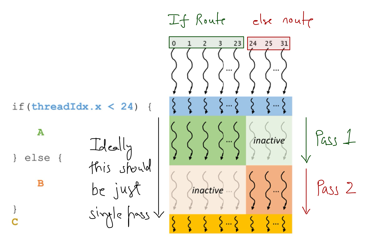
When threads in the same warp follow different execution paths, then it's said that the threads exhibit control divergence. It is also important to note that as the size of data increases, the performance impact of thread divergence decreases. For example, in vector addition:
- When the vector size is 100, 1 of the 4 warps will have control divergence, i.e., it affects 25% of the execution time.
- When the vector size is 1000, only 1 of the 32 warps will have control divergence, i.e., it affects ~3% of the execution time.
Warp Scheduling and Latency Tolerance
From the knowledge of the GPU hardware (that we have acquired so far), it looks like the loss in performance for matrix multiplication with small matrix sizes (Figure 1) is mostly due to the global memory accesses. However, this does not explain why the execution time does not increase with the increase in the matrix size. I mean that with large matrices, the number of global memory accesses also increases, but the execution time (for GPU) remains almost the same! GPUs can do this because the hardware is capable of latency tolerance or latency hiding.
There are usually more threads assigned to an SM than its cores. This is done so that GPUs can tolerate long-latency operations (like global memory accesses). With enough warps, SM can find a warp to execute while others are waiting for long-latency operations (like getting data from global memory). Filling the latency time of operations from some threads with work from others is called latency tolerance or latency hiding. The selection of warps ready for execution does not introduce any computational cost because GPU hardware is designed to facilitate zero-overhead thread scheduling.
That's why, for large matrices, more warps are available to hide the latency due to global memory accesses. There is a limit (set by CUDA) to the number of warps that can be assigned to an SM. However, it's not possible to assign an SM with the maximum number of warps that it supports because of constraints on execution resources (like registers and shared memory) in an SM. The resources are dynamically partitioned such that SMs can execute many blocks with few threads or a few blocks with many threads.
For example, an Ampere A100 GPU can support
- 32 blocks per SM
- 64 warps (2048 threads) per SM
- 1024 threads per block
So, if
- A grid is launched with 1024 threads in a block (maximum allowed)
Ans. Each SM can accommodate 2 blocks (with 2048 threads total, matching the maximum allowed per SM).
- A grid is launched with 512 threads in a block
Ans. Each SM can accommodate 4 blocks (with 2048 threads total, matching the maximum allowed per SM).
- A grid is launched with 256 threads in a block
Ans. Each SM can accommodate 8 blocks (with 2048 threads total, matching the maximum allowed per SM).
- A grid is launched with 64 threads in a block
Ans. Each SM can accommodate 32 blocks (with 2048 threads total, matching the maximum allowed per SM).
A negative situation might arise when the maximum number of threads allowed per block is not divisible by the block size. For example, an Ampere A100 GPU can support 2048 threads per SM
So, if
- A grid is launched with 700 threads in a block
Ans. SM can hold only 2 blocks (totaling 1400 threads), and the remaining 648 thread slots are unutilized. The occupancy in this case is 1400 (assigned threads) / 2048 (maximum threads) = 68.35%.
Query Device Properties
The Compute capability of a GPU indicates the amount of resources available (generally, larger compute capability means larger compute resources). We can find out the available resources for a GPU using the following commands:
- Number of available GPUs:
cudaGetDeviceCount()
int dev_count;
cudaGetDeviceCount(&dev_count);- Device properties of a GPU: All available GPUs are numbered
0todev_count - 1. API functioncudaGetDeviceProperties()can be used to get the properties of a select GPU.
cudaDeviceProp dev_prop;
for(unsigned int i = 0; i < dev_count; i++)
{
    cudaGetDeviceProperties(&dev_prop, i);

    // Further details of different properties
    .
    .
    .
}
For the select device (in the loop), we can get the following device properties:
- Max number of threads allowed in a block:
dev_prop.maxThreadsPerBlock - Number of SMs in the GPU:
dev_prop.multiProcessorCount - The Clock frequency of the GPU cores:
dev_prop.clockRate - Max number of threads allowed in each dimension of a block:
- X Dimension:
dev_prop.maxThreadsDim[0] - Y Dimension:
dev_prop.maxThreadsDim[1] - Z Dimension:
dev_prop.maxThreadsDim[2]
- X Dimension:
- Max number of blocks allowed in each dimension of a grid:
- X Dimension:
dev_prop.maxGridSize[0] - Y Dimension:
dev_prop.maxThreadsDim[1] - Z Dimension:
dev_prop.maxThreadsDim[2]
- X Dimension:
- Number of available registers in each SM:
dev_prop.regsPerBlock - Warp size:
dev_prop.warpSize
Conclusions
Now that I've explained the details related to the GPU architecture. I will summarize everything by answering the questions asked at the start of this blog post.
- What is the architecture of a modern GPU?
Ans. A modern GPU has three main components: Streaming Processors (CUDA cores), Memory, and Control. CUDA cores are grouped into multiple Streaming Processors, and memory is divided into registers, shared memory, and global memory.
- What are the different memory types in a GPU?
Ans. There are five types of memory in a CUDA device: Global Memory, Local Memory, Constant Memory, Shared Memory, and Registers.
- How do CUDA blocks/threads work with different GPU hardware components?
Ans. When a kernel is launched, all threads in a block are simultaneously assigned to the same SM. Once a block is assigned to an SM, it is divided into 32-thread units called warps. There are usually more threads assigned to an SM than its cores. This is done so that GPUs can tolerate long-latency operations (like global memory accesses).
- What are the common coding practices to get the best out of a GPU?
Ans. SIMD execution on a warp suggests that for optimum results, all threads in a warp must follow the same execution path or control flow, i.e., there should not be any control divergence of threads.
- Is there a way to determine the resources available for a GPU?
Ans. Several commands (predefined CUDA functions) can be used to determine the available resources for a GPU.